The Cost of Mistakes on Parts

Creating a proper schematic symbol and PCB footprint for a new part and meticulously checking it for errors can be a tedious task. But when you don’t have a trusted, verified parts library this task is exceptionally necessary due to what you’re risking if you don’t buckle down and verify yourself. A mistake in your part design can be very costly. We consulted a reputable manufacturer, Hooman Javdan from Circuits Central Inc., on the types and ranges of costs that result from part design errors. Let’s analyze what types of costs a mistake on parts could incur for you and your company.

Material and Equipment Cost

The most obvious cost, and possibly the worst case scenario is the cost of re-spinning more boards. If the paste mask is wrong a new stencil will cost in the hundreds of dollars. A new stencil will also extend the timeline of the project by a few days so the manufacturer has enough time to have it made. If the board is just plain wrong, fabbing and assembling a new batch of boards can cost in the thousands.If a particular component’s origin is incorrectly displaced off-center in a part design, then the pick-and-place machine will attempt to put the part on the wrong spot on the board. This will result in part losses, so the cost depends on which part is being improperly placed. If the part in question is a processor, an FPGA, a memory module or something similar, it can be a very costly mistake.

Rework costs can vary wildly in terms of both dollars and time. If a pin marking on the silkscreen is wrong, or possibly flipped because it is on the back of the board, then a part may need to be manually removed and resoldered correctly. For simple parts this may cost only a few minutes per board and a total of 1 day of delay. For more salvaging and reworking more expensive parts, such as a BGA, this may mean spending hours on each board to remove, clean, reball and resolder each BGA and take around a week in total. Expect to pay around $300 per hour for your rework time, making this an important costly decision.

For a small batch of prototype boards (5-10 boards), expect a re-spin to cost in these ranges:

cost-mistake-parts-table

The cost of PCBs are driven up by increased set-up time for the manufacturer due to higher component counts, higher parts costs for expensive ICs like processors or FPGAs, parts that require an conformal coating and thus curing time, and complex mechanical assemblies.

Testing & Debugging Cost

If a symbol or footprint has an error, any resulting malfunctions can take a long wild goose chase to track down the root cause. Hours and days of engineering time can be wasted before it’s determined that the malfunction is as a result of an unverified part design. If a part is placed in the wrong orientation, it could drive high current through a part of the board and damage further components on it. You might not notice this problem until you’ve noticed the cascade of damage on the board. These boards could initially pass quality control and then provide a challenging debug project for an engineer, or fail to work properly in the field. Assuming that engineering time costs companies around $50-100 per hour, it is definitely a huge financial risk to have engineers spending their time on debugging instead of on designing.

Expediency Cost

Usually, a small batch of prototype boards can be completed by a manufacturer in around 2 weeks. However, when an error is found and a re-spin is ordered, companies often want to avoid waiting another two weeks and will have their next batch of boards expedited. If you’re expediting from 2 weeks to 24 hours, expect to pay double for the second batch of boards.

Time to Market Cost

The alternative to paying expediency costs is to delay the launch of the project by a few weeks or months. The cost of the delay depends widely on your market and on your competitors, but it can easily become unmanageably large. Consider that many markets have seasonal milestones they must hit with their products, whether they are targeting a launch at a specific industry conference or trade show or whether it’s a large consumer electronics company trying to hit the Christmas deadline. These market windows must be hit.

There are several things to consider when evaluating the time to market cost, but know that it typically results in an increase in sunken research and development cost, a decrease in sales life, and a loss of market share.

cost-mistake-parts-graph

You can find many calculators online that can help you determine the cost of going late to market, but a general optimistic estimate would be 2% of total profit is lost for every month a product is delivered late.

So if you shudder at the thought of throwing money away needlessly, know that using verified parts is far from needless – it’s essential.

Creating the Perfect Part (4/4)

If you need to make use of a component and it is not already in the parts library, what two things do you need to consider while designing it in your CAD tool?

  • How to make your part reusable in the future
  • How to make your part design practical for fabrication

The last part aspect worth perfecting, is the footprint of the part.  The footprint is used to describe the specific mechanical shape of the component.  The perfection of this aspect is crucial for the PCB layout design to ensure manufacturing goes smoothly.  This last entry in our Perfect Part series focuses on optimizing our design for manufacturing considerations.

We contacted Hooman Javdan from Circuits Central Inc., a manufacturing expert of more than 5000 designs, for his best practices on designing a footprint that will best position your layout design for a successful fabrication process.

There are some best practices to use while inputting the exact dimensions of your footprint.

  1. It is important to make sure the units that are used in the data sheet are the same units you’re using to design the part – avoid converting between metric and imperial yourself.
  2. For through-hole and surface mount components, the hole and pad size need to be chosen correctly.  Consult the IPC standard 7351 (here) and follow the guidelines for the component you’re creating.
  3. Likewise, for through-hole components that need thermal spokes, the spoke width should be set according to the manufacturer’s capability.  Your manufacturer will give you guidance on the maximum surface area of the copper spokes, which will in turn help you choose the spoke thickness.

perfect-part-4-thermal

It is important to have pad sizes chosen perfectly, and this takes careful consulting of the data sheet and some experience.

  1. If a pad is designed too large, parts can be pulled to one side of the landing area during soldering and not connect on the other side.  The effect is called “tombstoning”
  2. The choice between Solder Mask Defined (SMD) and Non Solder Mask Defined (NSMD) for Ball Grid Array (BGA) parts is an important one.  For standard BGAs it is okay to use SMD, but for parts with a fine pitch, such as a Quad Flat No-leads package (QFN), it is important to use NSMD.  SMD will usually protect better against pad lifting, while NSMD will protect better against connection bridging.  See here for a comparison.
  3. Know that having a via-in-pad can make the pads effectively larger and cause some problems.

perfect-part-4-chip

According to Mr. Javdan, solder mask layer errors can be frustrating and costly.  If a BGA has an issue, the fabricator must remove the BGA, check its functionality, reball it, clean the board and solder it back on by hand which costs them time and you hundreds of dollars per board.  So be mindful of the manufacturing process in your designs.

For the practical “How-To” of creating the layout footprint of a new component in Upverter, see our YouTube video.

Creating the Perfect Part (3/4)

Part 3 – Footprints

If you need to use a component that’s not in your library, what two things do you need to consider while designing it in your CAD tool?

  • How to make your part design accurate and practical for manufacturing
  • How to make your part reusable in the future

The last part aspect worth perfecting, is the footprint of the part.  The footprint is used to describe the specific mechanical shape of the component.  The perfection of this aspect is crucial for the PCB layout design to ensure manufacturing goes smoothly.  We will split discussion of the footprint into two pieces, and this piece focuses on optimizing the readability of our silkscreen in our design.

Footprint

There are a few footprint design tips that will get you more usability for your part in future projects.

  1. Ensure the package outline exactly matches the outline of the component (use the nominal size from the data sheet).  This helps you be aware of size of the actual body of the package during PCB layout so you can position it correctly on your board.  This is especially useful for placing connectors whose body position on the board must be precise.
  2. Have the package outline centred around (0,0) on the design grid so that if the part is rotated it doesn’t also drastically change position.  The part origin is where pick and place machines will grab the part during assembly so an exception to this rule is if you need to move the part origin to an area with a smooth surface.
  3. Also for usability of the design, it is important to have the Pin #1 of the part, or the positive pin of a two-pin polarized part (like a diode), marked on the silk screen.
perfect-part-3-bga-footprint


The silkscreen design of our footprint needs to consider the actual fabrication and manufacture of the board itself.   We contacted Hooman Javdan from Circuits Central Inc., a fabrication expert of more than 5000 designs for his advice on designing a footprint that will actually result in the PCB you want. One example he gave was that when marking pins on the silk screen (such as for Pin #1 or marking polarity in unidirectional parts), make sure that the marking is not under where the actual component is going to be placed so that it remains visible after the component is mounted.  This sounds obvious but you’d be surprised how many designers make this mistake by accident.

Like This!

perfect-part-3-bga-correct-marking


Not Like This…

perfect-part-3-bga-incorrect-marking


Likewise, any part that has a grid array of pins (like a BGA) should have silk screen markings on the opposite side of the board indicating row and column so that someone probing a particular via can understand which BGA where to place their probe.  If you find that you’re doing this often with a part, it might make sense to include this back-side silkscreen design as part of your component design.  You can shift and adjust the back silk screen markings based on which way the via-in-pads go.

According to Mr. Javdan, the silk screen placement has some tolerance and will often be slightly misaligned.  If precise silkscreen locations are important to you, ask your PCB fab about their silkscreen tolerances so you can plan ahead.

Stay tuned for the next and final part of our “Perfect Part” series where we will focus on how perfecting the footprint of your component design will help you optimize your design for manufacturing considerations.

For the practical “How-To” of creating the layout footprint of a new component in Upverter, see our YouTube video.

Creating the Perfect Part (2/4)

Part 2 – Schematic Symbols

If you need to use a component that’s not in your library, what two things do you need to consider while designing it in your CAD tool?

  • How to make your part design accurate and practical for manufacturing
  • How to make your part reusable in the future

The second part aspect that requires perfection, and the focus of part 2 of our series, is the schematic symbol which is a logical (non-physical) representation of the part that emphasizes readability for the design engineer’s schematic.

Schematic Symbol

The main goal in designing the schematic symbol is to preserve clarity of the overall schematic, and to make your representation of the part helpful in accomplishing that.

1) Consider breaking up a part into multiple symbols, like a dual op-amp.

perfect-part-2-dualopamp


2) For ICs, their schematic symbol (typically a square) should be as large as necessary to be readable.

Like this!

perfect-part-2-readable


Not Like This…     

perfect-part-2-notreadable


3) It is better to avoid using pins on the top or bottom of the symbol, and that a left-to-right flow should be preserved (inputs on the left, outputs on the right).

Like this!

perfect-part-2-sidepins


Not Like this….

perfect-part-2-incorrectpins


4) Pins should be named in such a way that they indicate their function and uppercase letters should be used.

5) For clarity, all of the chip’s pins should be shown.  Pins that are unused should still be shown, but marked as such on the schematic (typically with a no-connect flag that looks like the letter ‘X’).  The thermal pad should have a pin on the symbol and should be connected to ground in the schematic.

This Arduino Micro, for example.

perfect-part-2-arduino-micro


Consult Upverter’s style guide (here) for more suggestions on how to keep your schematic symbols and nets clear and readable.

For the practical “How-To” of creating the schematic symbol of a new component in Upverter, see our YouTube video.

Creating the Perfect Part (1/4)

This is Part 1/4 in an Upverter Blog series on creating the perfect part.

Most hardware designers, in their unique and innovative designs, encounter the problem that the part they want to use isn’t already included in their design software’s libraries.  In certain design programs, adding a new part can be tedious work.  Making a mistake can be very costly during manufacturing.  Furthermore, you may want to reuse the part in the future.  Thus it is worthwhile to spend the time to ensure that your part creation is “perfect”.

If you need to use a component that’s not in your library, what two things do you need to consider while designing it in your CAD tool?

  • How to make your part design accurate and practical for manufacturing
  • How to make your part reusable in the future

There are three important aspects that require a hardware designer’s attention to ensure part perfection.

The first, introduced below, is the part attributes, which contain relevant functional and reference information to explain to the basics about that part.  We’ll go into more detail later on exactly what information should be contained in there.

The second, and the focus of part 2 of our series, is the schematic symbol which is a logical representation of the part that emphasizes readability for the design engineer’s schematic.

The last aspect, is the footprint of the component, which is used to describe a specific mechanical shape of the part and is necessary for the PCB layout and manufacturing.  We will split discussion of the footprint into two parts, optimizing our design first for the layout design and then for manufacturing considerations.

Attributes

The attributes should contain a few obvious but important notes.

  1. The full part number of the product you want to use should be included as well as the name of the manufacturer of the part.
  2. A URL to the part’s datasheet.  This can help someone quickly locate the information that was used to create the part in the part library.
  3. The package type (such as QFN, BGA, through-hole, etc.).
  4. Also to be included are any specifications necessary to understand what the part does.  For example, if the part is a crystal oscillator, the attributes should indicate the frequency it operates at.
perfect-part-1


For the practical “How-To” of creating the attributes of a new component in Upverter, see our YouTube video.

How to Price Your HW Product (5/5)

Part 5 – Profit.

If you’re building a HW product, you’ve inevitably wondered:

  1. How much can I sell it for?
  2. How much money can I make?

In the final part of this 5 Part series, Alan Povall from Product Nimbus breaks down the exciting topic of Profit.  Take a read and leave your comments below!

Part 1 – The physical product (the stuff you hold in your hands)

Part 2 – Manufacturing and testing (making the stuff)

Part 3 – Packaging and Shipping (sending the stuff)

Part 4 – NREs (hidden costs that can sneak up on you)

Part 5 – Profit (everyone’s favourite!)

Profit

The last factor you need to consider in this model is profit, or more specifically how much profit you can make.

As you know, profit is ultimately determined by:

  1. How much your product costs to manufacture, minus margin / mark up.
  2. What the final retail price will be.

The final retail price (e.g. what your end customers actually pay) is in turn is tied to the customer / user research you should have carried out already. By now you should know:

  1. How much competing, similar or alternative products are selling for.
  2. How much your customers are willing to pay based on what they’ve told you (through discussions, pre-sales, faux-presales, cost-of-issue analysis, etc).

If you can’t answer the above two questions, drop everything and go find some customers to talk to. Yes, really. I’ll wait. It’s that important.

If you know what your end retail price should be (even as a range), then you can consider the sales model you’ll be using:

  • Direct Sales – you manufacture and sell directly to your customers. There are no real middle men. You are responsible for your sales channels / efforts, but can take much higher margins. Often a natural progression of this model is to sell directly to retailers, in order to reach a larger market.
  • Indirect Sales – you manufacture then ship product to distributors, who in turn ship to retailers (or depending on how niche your product is, you may ship straight to retailers). Both wholesalers & retailers add mark ups to your product (cutting into your profit margin), but take responsibility for promotion of your product and are often able to reach a wider audience.

If using indirect sales, there’s just one other major thing to remember: Margins.

  • Wholesalers typically have profit margins in the range of 20 – 50%.
  • Retailers typically have profit margins in the range of 10 – 40%. These vary wildly depending on whether they are online retailers (e.g. Amazon), boutique physical stores or large brick-and-mortar stores (e.g. Walmart). Large retailers are a completely different ball game, so be careful.

Both of these models have their own advantages and disadvantages, so I highly recommend spending some time getting to know the nuances so you know which one is right for you. Don’t skimp out on this. It can make or break your business, so invest some serious time here understanding which is best for your specific situation.

Margin from intermediaries need to be added on top of the profit you wish to make from your product. You need to be careful though that once everyone has taken their slice of the pie, you don’t end up with a retail price far beyond your customers’ expectations.

As a quick final note, beware the difference between profit margin and markup. Some people like to use them interchangeably, but they are two very different things. The crux of the difference is this:

  1. Profit margin is how much of your selling price (revenue) is actually profit, after to your costs (CoGS, Cost of Goods Sold) have been taken into account. Essentially, Profit Margin = (Revenue – CoGS) / Revenue
  2. Mark up is what percentage of your costs (CoGS) your profit is. Here’s some more maths: Mark Up = (Revenue – CoGS) / CoGS
  • For example: if you sell your product directly to customers for $100, and costs $35 to manufacture and distribute, then:
  • Your profit margin is: ($100 – $35) / $100 = 65%
  • Your markup is: ($100 – $35) / $35 = 185% (sounds like a lot, but it’s so-so)

So there you have it, a breakdown of where your money actually goes during manufacturing and how it affects your final retail price! 

Alan Povall is the Founder of Product Nimbus, which provides business resources for hardware tech start ups. Alan’s been involved with heavily in product development for over 7 years as part of an international HW design consultancy. He now works with aspiring entrepreneurs, start ups and even the odd charity to get their product ideas off paper and into the wild.

6 Steps to Verifying a Part you Didn’t Make

Saving time on your projects is what pre-populated parts libraries are all about, and they’re great at it.  But doing these quick checks will keep you confident that using parts you didn’t make are what you expect them to be.Ever heard your boss, or someone else in your industry mention the line “do a sanity check”?  I’ve also heard the term “do a smoke test”, or “run a warm/fuzzy test”.  To me, the “sanity check” line is a bit dramatic and implies your mental well-being is at stake, but in hardware design, these tests can mean the difference between being mildly upset over a part not being entered correctly in the library and losing hours of work or potentially thousands of dollars in fabrication costs.In an interview with Circuits Central’s Hooman Javdan, a contract manufacturer and PCB assembler of more than 5000 designs, he mentioned that selecting the wrong part or providing the wrong footprint for a specific application can mean hours lost and hundreds of dollars in remanufacturing cost overruns.

So before committing blindly to a complex part that you found already existing in your part library and doing a quick “cha-ching” in your head, it’s valuable to slow down and take a second look to make sure the part you’re selecting is really the part you think it is.  If the part attributes were properly populated and there is a URL to the data sheet, open it up and make sure it matches the data sheet of the part you’re hoping to use.  You’ll want to check both the schematic and the footprint against this data sheet next.  The good news is that a sanity check on a footprint can be done very fast with a bit of practice.

Some things you can quickly check on the schematic:

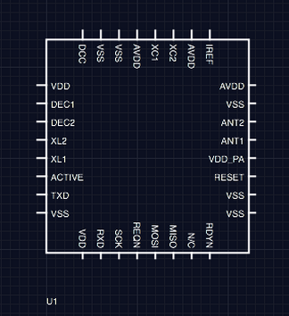
1) That the number of pins matches the number of pins on the data sheet.

2) That the names correctly match the pin designations in the data sheet.

With the footprint, you need to check the mechanical details against the data sheet.

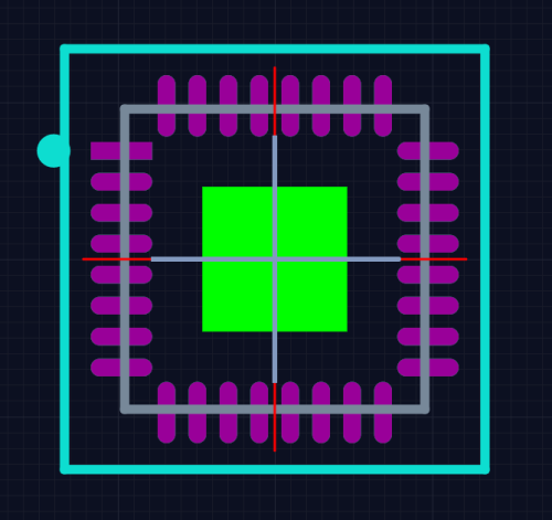
3) Use your hardware design tool’s measurement tool to measure the package outline and compare that to the size of the device in the data sheet.

image

4) The pad pitch or the pin pitch needs to match the data sheet too so measure those as well.

Note, ‘pitch’ means centre-to-centre spacing between adjacent pads and/or pins.

image

5) Measure the pad size, both length and width and ensure they seem reasonably larger than the pads on the part you’re using.

image

6) Make sure the pin numbers match, and that pin #1 is in the position you expect it to be.

image


If you have any other details you like to check as part of your ‘Sanity Check’ let us at Upverter know!  We’d love to hear from you.

These might seem like mundane details to check, but in the event that the part you’re using in your design software doesn’t exactly match the part you’re using in fabrication, checking these details means you likely won’t run into any issues anyways. If you can do these really fast checks that cover ~90% of the aspects of a part, you might spend a few minutes to save hours and sleep better at night with a warm/fuzzy feeling in a smoke-free environment, thus preserving your sanity.

How to Price your HW Product (4/5)

Part 4 – NRE’s: The Sneaky Costs.

image

If you’re building a HW product, you’ve inevitably wondered:

  1. How much can I sell it for?
  2. How much money can I make?

In Part 4 of this series, Alan Povall from Product Nimbus breaks down NRE costs.  These are often overlooked and can be surprising.  Take a read and leave your comments below!

Part 1 – The physical product (the stuff you hold in your hands)

Part 2 – Manufacturing and testing (making the stuff)

Part 3 – Packaging and Shipping (sending the stuff)

Part 4 – NREs (hidden costs that can sneak up on you)

Part 5 – Profit (everyone’s favourite!)

NRE Amortization:

Here’s one I love because so many people overlook it. NREs (Non-Recurring Engineering / Expense) usually come from four main places:

Design & development costs:

Electronics, software, industrial design, mechanical tests, IP, prototypes, user research, the works. Everything it cost you (or will cost you) to get a fully manufacturable design, but isn’t part of the physical per-unit cost itself.


Manufacturing set up:

Essentially the cost to get everything up and running for manufacturing, which is typically a flat fee from the manufacturer (depending on how well organized you are). It includes reviewing design files (if you have a good CM), setting up pick & place machines, getting stencils made and more. Typically put this value at $3,000 – $5,000 for a Western manufacturer, although it depends on the agreed upon conditions (e.g. it could be rolled it into the per-unit cost and tied to order volumes). There is often also a smaller per-batch set up fee (to get SMT reels loaded, stencils ready, AOI files loaded, etc).

Certifications:

FCC, UL, CE, FDA, Ex, etc all add up and vary depending on your product as well as the category it falls under, whether it is designated as a medical device, has RF transmitting capabilities and more. Standard certifications are in the $10k – 20k range if you do them right the first time. If you use pre-approved parts (or go through some of the Asian labs), that cost can be as low as $1,000. Failing the tests and having to resubmit can drive up cost, depending on the certification being pursued.  It’s a good idea to start discussions with a certification lab once you have a prototype so you can catch early problems.

Enclosure production cost:

If you are using 3D printing for small volume runs, then one-off costs are less of an issue. However if you are using injection moulding for instance, then the cost of having the mould created can be significant and needs to be taken into account. Depending on the actual mould complexity and where you get them made, these can range anywhere from $3,000 to $12,000 (or more).

Test Fixtures:

You may need some sort of test fixture in order to carry out functional tests to ensure that the electronics (and mechanical bits) of your product are working before putting everything into a box to ship. These can range from simple manually operated fixtures which take a few hundred dollars (or less) to create, through to complex ATEs (Automated Test Equipment) which are essentially a full product in their own right. ATEs can range anywhere from $15,000 – $50,000 (yes, really), depending, yet again on product complexity. The more complex a product is the longer manual testing will take, which means that as volume increases there will be a crossover point where manual labour becomes more expensive than creating and using an ATE.

The Key to Remember:

These costs need to be recouped throughout production (preferably sooner rather than later), and so need to be split across the anticipated production volumes. If your total development, manufacturing, enclosure and test fixture NREs are $250,000 (hypothetically) and your anticipated annual volume is 10,000 units, the amortized NRE cost as a per unit cost would be $25 per unit ($250,000 ÷ 10,000) on top of the other per unit manufacturing costs we’ve mentioned already. Naturally you could spread this over 2 or even 3 years (although that would be pushing it a bit), which would reduce the per unit cost to $12.5 and $8.33 respectively, depending on the accuracy of your sales projections (pro tip: they don’t climb exponentially).

Alan Povall is the Founder of Product Nimbus, which provides business resources for hardware tech start ups. Alan’s been involved with heavily in product development for over 7 years as part of an international HW design consultancy. He now works with aspiring entrepreneurs, start ups and even the odd charity to get their product ideas off paper and into the wild.

Upverter Workshop – Bluetooth Throwie

image

Here’s some information that should be of some help during the Upverter Workshop.

1: Setting up your account

2: Forking the Workshop Design

After logging in, check the link below. You’ll find the BTLE design we’ll be working with. In the right side bar labelled ‘issues’, there are some tips on what to do.

https://upverter.com/pch/5cba5ae5ee52b315/Waterloo-Hackathon-Weekend—Upverter-Workshop/

3: Building your design. 

When searching for modules in the Parts Library, make sure to search for “CC2541 under the ‘modules’ tab. You’ll find the three tools you’ll need for the workshop:  CC2541 Power Supply | CC2541 Bluetooth LE | CC2541 Accelerometer

image

4: Connecting the Circuit.

Okay. So you’ve finished inserting your modules. Now you’ve got to connect them!

Under the PCB Layout section, select the copper, line up your parts correctly, and that’s all! You’ve just created a lightweight bluetooth device!

Here’s a Link to the Slideshow.

Follow along the workshop, and call us over if you need anything.

How to Price your HW Product (3/5)

Part 3 – Packaging & Shipping

image

If you’re building a HW product, you’ve inevitably wondered:

  1. How much can I sell it for?
  2. How much money can I make?

In Part 3 of this series, Alan Povall from Product Nimbus explains why hardware startups shouldn’t worry about having packaging that’s as sexy as the iPhone.

How important are packaging and shipping?

Part 1 – The physical product (the stuff you hold in your hands)

Part 2 – Manufacturing and testing (making the stuff)

Part 3 – Packaging and Shipping (sending the stuff)

Part 4 – NREs (hidden costs that can sneak up on you)

Part 5 – Profit (everyone’s favourite!)

Packaging:

Packaging costs also vary widely depending on the quality of packing you want to wrap your shiny product in. It’s all the rage these days to go for ultra high quality packing design and materials to create a luxurious ‘unboxing’ experience. It’s my personal opinion that as a start up, your money should be spent on:

  1. Validating the living heck out of your market
  2. Creating a product experience so sublime that melts your customers brains into goo
  3. Finding the perfect manufacturing partner
  4. Promoting your product until you’re blue in the face

As you can tell from the above list, designing a 15 piece interlocking, shiny double bonded UV resistant cardboard portmanteau is not on the list. I’m not saying shouldn’t package your product beautifully (if you can do it for the right price), but I think you need to think very carefully about where your money goes. High end packaging can be anywhere from $5 – $20 per unit. Basic but respectable packing can start at $0.30 – 1.00 per unit.

Shipping:

Shipping costs are another fun variable, which change considerably based on where you are shipping from, your manufacturer’s MoQ and how Just-In-Time your sales model is. In most cases it’s not feasible to use air freight (unless your volumes are still relatively low), which means you’re stuck with a combination of sea and land transport. It’s an aspect that’s often overlooked with the Asian manufacturers, as they have large MoQs (up to 3,000 – 5,000), which need to be shipped to USA / Europe in most cases (not to mention port clearance fees), weeks if not months ahead of when you think you’ll actually need the stock.

If you know the weight, dimensions and MoQ your product to be made, you can phone around and get some shipping / clearance fee estimates from shipping companies.


Alan Povall is the Founder of Product Nimbus, which provides business resources for hardware tech start ups. Alan’s been involved with heavily in product development for over 7 years as part of an international HW design consultancy. He now works with aspiring entrepreneurs, start ups and even the odd charity to get their product ideas off paper and into the wild.